Signed in as:
filler@godaddy.com
Signed in as:
filler@godaddy.com

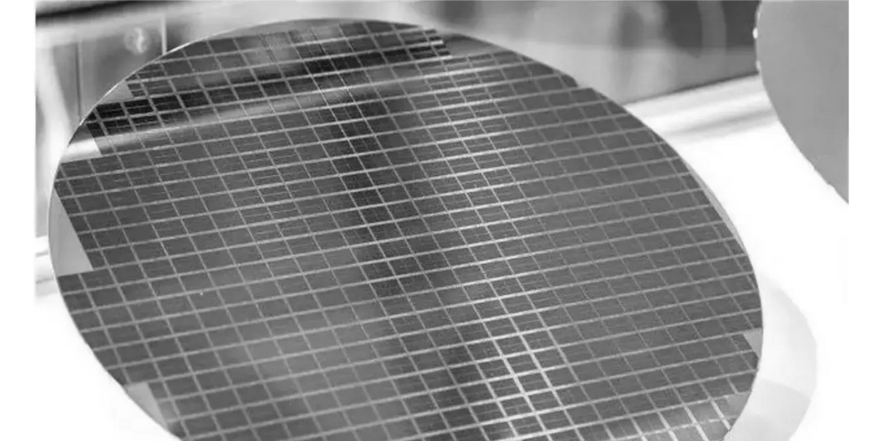
NanoFort Group provides high-performance wide bandgap (WBG) and III-V compound semiconductor substrates specifically engineered for the most demanding next-generation power electronics, high-frequency RF applications, and advanced optoelectronics. These materials represent a significant leap in semiconductor technology, offering vastly superior thermal conductivity, significantly higher breakdown voltages, and faster electron mobility when compared to traditional silicon-based substrates.
By utilizing these advanced properties, our substrates enable the development of smaller, faster, and more efficient components that can operate reliably under extreme temperatures and high-voltage conditions. This makes them the definitive industry standard for critical infrastructure and emerging technologies, including electric vehicle (EV) powertrains, 5G telecommunications networks, and sophisticated aerospace systems. We work closely with leading global foundries to ensure that our SiC, GaN, and GaAs materials meet the stringent purity and crystalline quality standards required to push the boundaries of modern power density and signal integrity.
We collaborate directly with manufacturers to offer extensive customization for our compound semiconductor range. Contact our team today to discuss how we can tailor these high-performance substrates to meet your specific project requirements.


NanoFort’s III-V and WBG materials are precision-engineered for ultra-low defect density and superior crystalline purity, ensuring the highest possible reliability for demanding power and high-frequency applications. By maintaining strict control over the epitaxial growth and substrate slicing processes, we deliver materials that exhibit exceptional thermal and electrical stability, which is critical for minimizing energy loss and maximizing device longevity.
Our high-purity substrates are trusted across Australia by leading aerospace and defense contractors, as well as pioneering renewable energy researchers, to provide the robust foundation needed for cutting-edge innovation. Whether you are developing high-efficiency inverters for solar arrays or advanced radar components, NanoFort materials ensure repeatable experimental results and the structural integrity required to perform in the most extreme operating environments.
We maintain local Brisbane inventory of our core compound semiconductor substrates, including SiC, GaN, and GaAs, to ensure your high-tech projects remain on schedule. Contact our team today for a bulk quote or place your order now for immediate dispatch across Australia.
© 2025 NanoFort Group Pty Ltd | ABN 88 694 192 053. All rights reserved.© 2025 NanoFort Group Pty Ltd
Privacy Policy | Terms of Sale | Returns Policy | Contact Us
We use cookies to analyze website traffic and optimize your website experience. By accepting our use of cookies, your data will be aggregated with all other user data.